
Key Features
- Pogo Plus design
- LFRE plating
- Flat and “Micro-Textured” tips
Bead Target Probes Product Line


Introduction – What is Bead Probe Technology?
Bead Probing is a methodology for placing test points directly on a PCB’s copper traces, or top metal, thus forming a “Bead Probe”. These Bead Probes are then contacted by “Bead Target Probes” during in-circuit testing for expanded test access. Bead probe testing was developed by a major board test ATE supplier. ECT is supporting this technology with OEM’s, contract manufacturers, and test fixture partners.
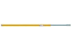
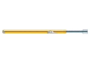
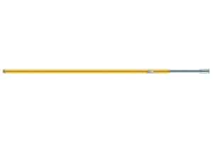
ECT has developed a series of spring probes, BTP and BPLT, specifically for Bead Probe applications featuring:
Pogo Plus Design
ECT’s Pogo Plus design is an excellent choice for Bead Probe challenges. The bias ball technology maintains excellent internal contact between the barrel and plunger even at the low forces required for bead probe applications.
LFRE Plating
ECT’s proven LFRE plating offers a significant increase in hardness over a typical gold plating hardness of 130-200 Knoop, providing a much higher range of 550-650 Knoop. LFRE plating is also less porous which results in a more durable surface that is less susceptible to solder and material transfer from Bead Probes.
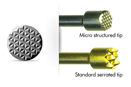
Flat and “Micro-Textured” Tips
The hemi-ellipsoid shape of a Bead Probe presents a unique probing challenge in that standard serrated probes may fall into the valleys between serrations. ECT has developed a new textured tip face that is optimized for contact to the hemi-ellipsoid shape of Bead Probe as small as .004.
An innovative “Micro-Textured” tip incorporates closely spaced triangular pyramid shapes to form a textured surface. Perfect for contacting beads that are long, yet have a small width when placed on a PCB trace.
Proven methodology, provides excellent in-circuit testing
- Provides excellent test access
- Beads can be placed directly on copper traces
- Eliminates the need for costly re-routing of signal paths
- Allows for more probing options
Applications
- In-circuit testing (ICT)